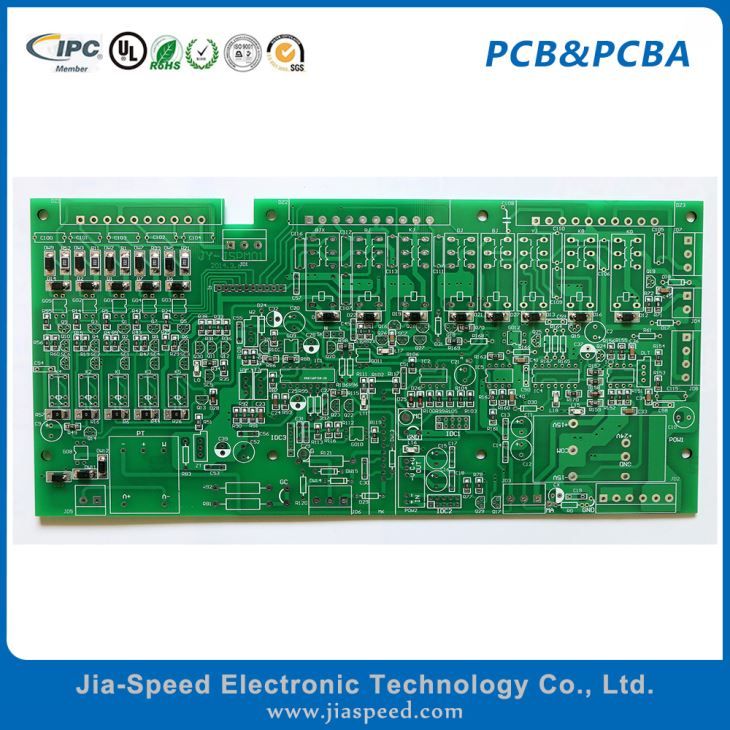

سعر فوب
أحصل على آخر سعر( Negotiable )
|100 Cubic Centimeter Minimum Order
بلد:
China
نموذج رقم:
HDI TG170
سعر فوب:
( Negotiable ) أحصل على آخر سعر
الموقع:
SHANXI,CHINA
سعر الحد الأدنى للطلب:
-
الحد الأدني للطلب:
100 Cubic Centimeter
تفاصيل التغليف:
CARTON/1PCS
موعد التسليم:
5-10DAYS
القدرة على التوريد:
50000 Set per Month
نوع الدفع:
T/T, L/C, D/P, Western Union
مجموعة المنتج :
-
الشخص الذي يمكن الاتصال به Yarina zhang
Xian, Shaanxi
Model
Number:10-layer HDI PCB
Number
of Layers:1-48 layer
Base
Material:FR-4
Copper
Thickness:0.25 Oz -12 Oz
Board
Thickness:1.8mm
Min.
Hole Size:0.004"
Min.
Line Width:2mil
Min.
Line Spacing:2mil
Surface
Finishing:Immersion Gold,ENIG
Solder
Mask:Green. Red. Blue. White. Black.Yellow
PCB
Assembly process:DIP. ICT PCB Assembly
HDI is an abbreviation of High Density Interconnector. It is a kind of technology (technical) for producing printed boards, and a circuit board with a relatively high density of wiring distribution using the micro blind buried hole technology. HDI is a compact product designed for small capacity users. It adopts a modular and parallel design, a module capacity of 1000VA (1U in height), natural cooling, can be directly placed into a 19 rack, and can be connected in parallel to a maximum of 6 modules. This product uses all-digital signal process control (DSP) technology and many The patented technology has a full range of adaptability to load and a strong short-term overload capability, regardless of load power factor and crest factor.
Advantages
1 Reduces PCB cost: When the density of the PCB increases more than eight layers, manufacturing with HDI will cost less than the traditional
2 complex lamination process.
3 Increase the line density: the interconnection of traditional circuit boards and parts
4 conducive to the use of advanced packaging technology

5 has better electrical performance and signal correctness
6 Better reliability
7 can improve thermal properties
8 Improves RF/Electromagnetic/Electrostatic Discharge (RFI/EMI/ESD)
9 Increase design efficiency
Characteristics:
Blind and/or buried vias
Via-in-pad
Through vias from surface to surface
20 µm circuit geometries
30 µm dielectric layers
50 µm laser vias
125 µm bump pitch processing
Our high density circuit boards have the technology-pushing capabilities to drive applications in a large number of industries including but not limited to semiconductor test equipment, defense, medical and aerospace.
JIA-Speed can provide you with the highest quality HDI PCB, please do not hesitate to contact us TEL: +8618729758649
| بلد: | China |
| نموذج رقم: | HDI TG170 |
| سعر فوب: | ( Negotiable ) أحصل على آخر سعر |
| الموقع: | SHANXI,CHINA |
| سعر الحد الأدنى للطلب: | - |
| الحد الأدني للطلب: | 100 Cubic Centimeter |
| تفاصيل التغليف: | CARTON/1PCS |
| موعد التسليم: | 5-10DAYS |
| القدرة على التوريد: | 50000 Set per Month |
| نوع الدفع: | T/T, L/C, D/P, Western Union |
| مجموعة المنتج : | - |